 July 27, 2024
Samsung
Samsung building advanced chip-packaging facilities
[ET NEWS] Samsung Electronics is ramping up investments in advanced chip packaging technologies, building a new manufacturing complex in Korea, according to industry sources on March 28.
The new complex will be using Samsung Display’s LCD panel production plant in Cheonan, South Chungcheong Province, to adopt advanced chip packaging technologies such as high-bandwidth memory and wafer-level packaging.
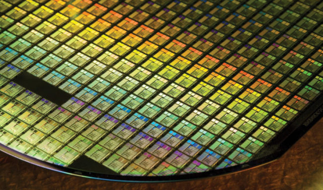 |
The HBM greatly improves power efficiency as it is increasingly being integrated into chips for artificial intelligence technologies. The 3-D WLP is used for imaging sensors of high-speed cameras in mobile devices like the current Galaxy S9.
Samsung plans to adopt 2.5D and Fan-Out packaging technologies at the new complex. Taiwan’s TSMC was the first to commercialize the Fan-Out packaging, adopting it to Apple’s A Series processors.
“Considerable resources are expected to be poured into equipment purchases. After completing the initial setting by the year-end, Samsung could seek expansion depending on demand,” an industry source told ET News on condition of anonymity.
Samsung, the world’s largest memory chipmaker and a foundry powerhouse that makes chips for outside clients, has been focusing on wafer processing thus far, while making little investments in packaging technologies.
But recently, demand for advanced packaging technologies is growing as they play a key role in integrating upgraded chips into smaller mobile and wearable devices or vehicles.
By Han Joo-yeop (powerusr@etnews.com)
This story was co-produced by ET News and The Investor.


