 April 17, 2024
Samsung
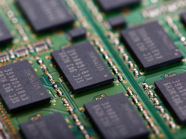
Samsung’s new semiconductor plant to go online in July
[THE INVESTOR] Tech giant Samsung Electronics will start operating its new semiconductor facilities in Pyeongtaek, Gyeonggi Province, from July, according to news reports on April 12.
The facilities are the world’s largest in size, built on 2.89 million square meters of land. The Korean tech giant will churn out fourth-generation 3-D NAND flash memory chips that stack 64-layers of cells vertically. The chipmaker has already asked its partners to supply necessary chip manufacturing equipment by the end of May, according to the Seoul Economy Daily.
 |
Related:
Samsung’s chip investment outstrips rivals this year
Samsung shares continue rally on back of brisk chip business
“Initially, the production volume at the new facilities will be limited and it will a couple of years before the facilities are fully operational,” said a source quoted by the publication.
Samsung is expected to start operations at the chip-making complex this year, but a specific timeline has not yet been officially released.
Construction started in 2015, costing the firm 15.6 trillion won (US$13.6 billion). The full production capacity for both planar and vertical NAND chips is estimated to stand at 450,000 wafers per month, with 3-D NAND chips accounting for more than half the volume.
Samsung is currently the world’s No. 1 NAND flash memory chip company. It saw its global market share increase from 32 percent in 2015 to 36.1 percent last year, according to market research firm IHS Markit.
By Kim Young-won (wone0102@heraldcorp.com)