
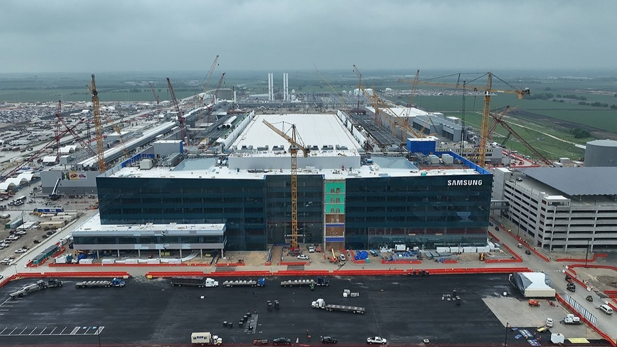
Samsung Electronics' $17 billion foundry under construction in Taylor, Texas, has moved into the equipment installation and commissioning phase, with 183 job openings posted at the site as of Thursday, according to the company's careers page and industry sources.
The positions span core process engineering roles in lithography, etching, deposition and chemical-mechanical planarization, along with metrology, infrastructure safety and fab planning functions. A review of the postings shows Samsung began recruiting in earnest at least two months ago, with the bulk of core process roles listed over 30 days prior.
More recent additions, including six cleanroom technician positions and six infrastructure risk prevention roles posted this week, point to preparations for initial wafer processing.
Samsung plans to directly employ around 1,500 workers at the Taylor site, drawing on both local hires and staff transfers from its existing Austin campus, industry sources said. Equipment vendors including ASML, Lam Research and KLA are expected to deploy a further 1,500 or more engineers for tool installation and qualification, bringing the combined on-site workforce to roughly 3,000 during the setup period.
The fab secured temporary certificates of occupancy for key sections earlier this year, and began testing EUV lithography equipment last month, according to the sources. Samsung has said the facility will target 2-nanometer production using its gate-all-around transistor architecture, with an initial monthly output goal of 50,000 wafers.
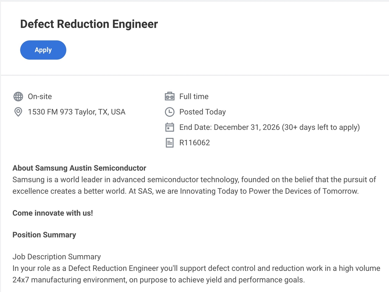
Several job descriptions, however, suggest operations will extend beyond cutting-edge nodes. One newly posted defect reduction engineer role lists responsibilities covering nodes from 45nm down to 14nm alongside foundry customer support, indicating the Taylor site may handle work linked to Samsung's adjacent Austin operations.
A capacity planning posting also describes a "1-to-3-year" horizon for coordinating tool installations and qualifying equipment, a timeline more conservative than the company's public target of trial runs this year and volume production in 2027.
Samsung received a $6.4 billion preliminary award under the US CHIPS Act in 2024 after committing to expand its Texas investment. The company is also hiring a director of Texas government relations, its highest-paying open position at the site, to manage policy engagement on incentives, utilities, water and energy, areas critical to sustaining a fab of this scale in central Texas.
By Moon Joon-hyun (mjh@heraldcorp.com)