
Wafers will stay in Korea, while advanced packaging and R&D move closer to US customers
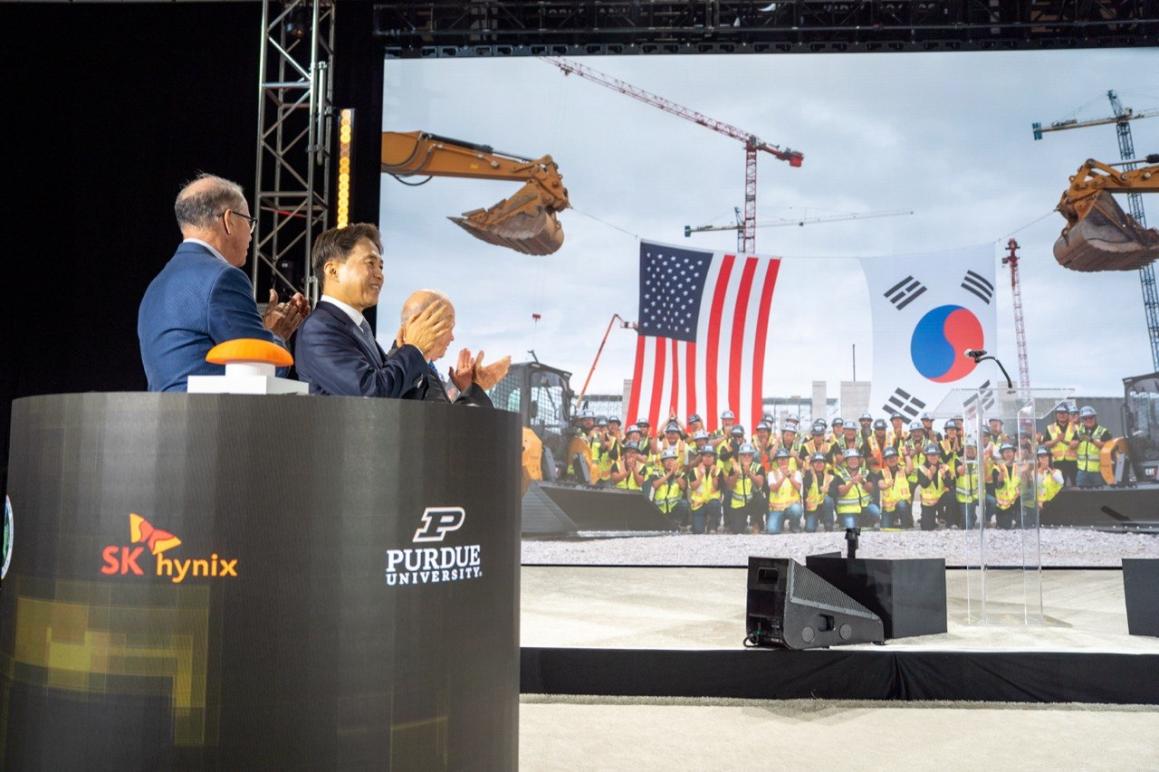
“The Indiana fab will become a gateway to deliver the first ‘Made in USA’ HBM products,” SK hynix CEO Kwak Noh-jung said at the groundbreaking ceremony on Aug. 26.
Those products, however, will begin in South Korea.
SK hynix will make the DRAM wafers at its Korean fabs, ship them across the Pacific and then stack, package and test them in West Lafayette, Indiana. The $4 billion-plus facility, the company's first HBM production base in the US, is due to begin mass production in the second half of 2029.
“The wafer is easy to move. The manufacturing ecosystem is not,” said Lee Jong-hwan, a professor of system semiconductor engineering at Sangmyung University.
Why the wafer stays in Korea
HBM, or high-bandwidth memory, begins as DRAM chips fabricated on wafers. Several of those chips are later stacked and connected into the high-speed memory package used alongside AI processors.
Making the wafers is the harder part to uproot.
SK hynix's Korean fabs sit amid experienced engineers, equipment makers, materials suppliers and infrastructure accumulated over decades. A new fab also has to go through the costly process of stabilizing production and improving yields before it can match an established line.
“There is little economic reason yet to duplicate in the US a production base whose competitiveness has already been proven in Korea,” said Kim Rok-ho, head of semiconductor research at Hana Securities.

SK hynix's spending at home points the same way. In August, the company approved 54.3 trillion won ($38.3 billion) for two new fabs through 2031: 35.2 trillion won for a DRAM fab in Yongin, Gyeonggi Province, and 19.1 trillion won for a NAND fab in Cheongju, South Chungcheong Province. It is separately building P&T7, a major HBM advanced packaging facility in Cheongju.
Moving the wafers between those Korean fabs and Indiana is also comparatively easy.
“Semiconductors aren't like cars, where every production process has to sit next to each other for logistics to work,” Lee said. “A wafer is small and light, while the value of what's on it is extremely high.”
So SK hynix can keep the most capital-intensive part of production where it already has scale, suppliers and manufacturing experience.
But that raises another question. If Korea can make the wafers and package HBM, too, why spend more than $4 billion to do part of the work in Indiana?
Why Indiana at all?
The answer begins with what packaging has become. “In HBM, packaging has become one of the core manufacturing processes that directly affects product performance and yield,” Lee said.
Indiana will not simply receive finished Korean chips and put them into boxes. Multiple DRAM chips must be stacked, connected and tested into the HBM package that works alongside an AI processor.
Next to that production line, SK hynix plans an Advanced Packaging R&D Testbed where customers, universities and business partners can make prototypes and validate performance. It is also working with nearby Purdue University on packaging research.

At the groundbreaking, SK hynix CEO Kwak described the US as the place where “top-tier customers, R&D capabilities, and partners align.”
For analyst Kim, that is the more important reason to be there.
“What matters is not getting the finished product to the customer a day earlier,” he said. “It is how quickly you can make a sample, test it and change it again when the customer changes its requirements.”
HBM is becoming more closely tailored to the processors it serves, bringing memory makers earlier into testing and qualification with AI-chip developers. SK hynix has not disclosed which customers will use the Indiana testbed.
Washington has its own reason for wanting that capability on US soil.
When the Commerce Department finalized SK hynix's CHIPS Act award, it described the project as filling a “critical gap” in the US semiconductor supply chain. The federal government committed up to $458 million in direct funding and up to $500 million in loans.
For now, the Indiana plant is designed to run on DRAM wafers shipped from Korea. SK hynix has announced no plan to build a US DRAM fab, while continuing to expand wafer production at home.
That makes any future US wafer investment a different kind of decision from the Indiana project, Lee said. The packaging plant does not need local wafer production to operate.
“Indiana can run with wafers made in Korea,” he said. “If SK hynix later decides it needs wafer production in the US as well, there would have to be another reason for it, whether that is capacity, customer demand, government policy or supply-chain risk becoming important enough to justify the higher cost.”
By Moon Joon-hyun (mjh@heraldcorp.com)